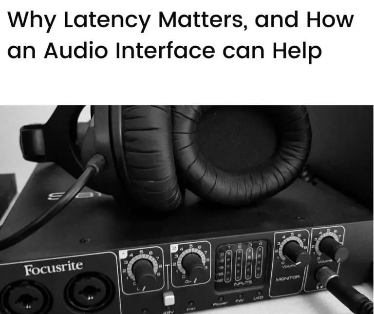
Analog-to-digital converters (ADC) are essential for bridging the analog and digital worlds and are used in a variety of applications. There are many types of ADC, each with its own history, merits, and limitations. And each has favored applications based on its strengths and weaknesses. In this article, we’ll look at the most widely used ADC configurations: what they are, how they work, and what they’re used for.
In this article we’ll look at:
- The most widely used types of ADC
- Delta-sigma ADC
- Flash or ‘parallel’ ADC
- Successive approximation (SAR) ADC
- Integrating ADC
- Conclusion
- FAQs
The most widely used types of ADC
The table below summarizes the most widely used types of analog-to-digital converters (ADC) and their strengths, weaknesses, and applications.
| ADC Type | Strengths | Weaknesses | Applications |
|---|---|---|---|
| Delta-sigma | High resolution and relatively inexpensive | Relatively slow and not suitable for high bandwidth applications | Precision DMMs, high-end data acquisition, pro-audio |
| Flash | Very fast | Large, expensive, and power-hungry | Fast digital oscilloscopes, video digitization, RADAR, wideband radio |
| Successive approximation (SAR) | Simple design, versatile | Not very fast, limited resolution, susceptible to noise | Industrial control and measurement, CMOS imaging |
| Voltage-to-frequency (integrating) | Precise, inexpensive, high noise rejection | Low accuracy | Remote sensing in noisy environments |
| Single-slope (integrating) | Good resolution | Low accuracy | DMMs and panel meters |
| Dual/multi-slope (integrating) | Relatively slow | Good accuracy | Precision DMMs |
Let’s look at these in more detail.
Delta-sigma ADC
We start by looking at delta-sigma ADC (also referred to as ‘sigma-delta ADC’)—a highly accurate and popular type of ADC, favored in many high-end applications, including professional audio applications.
These ADC are not very fast, but they are relatively inexpensive and support high resolutions—up to 32 bits—and make the most of both analog (fast) and digital (robust) circuitry. The delta-sigma approach is used in both ADC and DAC (digital-to-analog) applications.
A key to delta-sigma’s success is that only the changes (delta) in values between consecutive samples are transmitted rather than the absolute values of the samples—this results in high transmission efficiency.
Applications include precision digital multimeters (DMM), high-end data acquisition and communication systems, and (as mentioned) professional audio.
The concepts behind delta-sigma conversion
To understand how delta-sigma conversion works, you’ll need to be familiar with quantization noise, oversampling, digital filtering, and noise shaping.
Quantization noise
Quantization noise results from digitizing an analog signal. It’s caused by the loss of information (distortion) that occurs when converting a continuous signal to a discrete (i.e., digital) form.
The higher the bit-depth used for digitization, the lower the quantization noise. This is due to the increased ‘granularity’ that a higher bit-depth allows.
Oversampling
Oversampling is using a higher sampling rate than necessary when digitizing a signal.
According to information theory, a sampling rate of at least twice the (highest) frequency of an analog input signal should be used to prevent aliasing (a type of distortion)—this is known as the Nyquist rate.
So, oversampling refers to using a rate higher than the Nyquist rate.
Oversampling has the benefit of reducing the average quantization noise in the proximity (bandwidth) of a signal by spreading the noise energy over a wider frequency range than the Nyquist rate implies. This results in more energy for the digitized signal relative to its quantization noise, i.e., a higher signal-to-noise ratio (SNR).
Oversampling is usually done at a multiple of the Nyquist rate to maximize its benefits.
Digital filtering
Digital filtering refers to limiting the range of frequencies that pass through a system (i.e., filtering out unwanted frequencies) by using digital circuits.
When using oversampling, as mentioned, the average quantization noise is reduced by spreading it over a wider frequency range and improving the SNR.
By applying a low-pass digital filter to an oversampled signal (i.e., allowing frequencies below a certain threshold to pass), only the frequency range that includes the main (digitized) signal is retained, with an improved SNR, and the unwanted frequency range (containing noise) is filtered out.
So, by applying digital filtering after oversampling, a digitized signal within the desired frequency range and with a sufficiently high SNR can be produced.
Noise shaping
Other than oversampling, a higher bit-depth also reduces the quantization noise.
As it happens, there’s an approximate equivalence between oversampling by two times (2x) and a 0.5-bit increase in bit depth: both will improve the SNR by around 3 dB.
But this is before considering the impact of a technique known as noise shaping.
Noise shaping shifts most of the quantization noise to higher frequencies.
So, after applying noise shaping, the amount of quantization noise in the vicinity of the main (digitized) signal’s frequency is reduced as most of the noise shifts to higher frequencies.
After applying both noise shaping and oversampling, the SNR improvement is much higher than 3 dB for a 2x increase in oversampling—it can be as high as 9 dB or 15 dB, for instance, depending on circuit design.
Bringing it all together—how delta-sigma conversion works
Delta-sigma conversion exploits all the techniques discussed above to produce excellent results.
And in practice, a bit-depth of only 1 is used in many delta-sigma ADC.
Why only 1 bit?
Because it’s easy and inexpensive to build.
It also keeps the circuit design simple. Adding just one more bit, for instance, introduces a range of design complexities.
And we know that even 1 bit is enough to produce a high SNR due to the combined effects of oversampling and noise shaping.
Bringing it all together, the basic operation of a delta-sigma ADC is summarized below.
Basic operation:
- An input analog signal is converted to a bit-stream (typically 1-bit) by using an analog modulator
- Oversampling, noise shaping, and low-pass digital filtering are done to reduce the average noise, push the noise out of the bit-stream’s signal bandwidth, and filter out the noise
- Finally, decimation is applied (i.e., discarding samples beyond what’s required) to reduce the bit-stream’s high sample rate (due to oversampling) to a more usable data rate.
Pros:
- High accuracy and resolution
- Well suited to hi-fidelity audio applications
- Relatively inexpensive
Cons:
- Relatively slow
- Generally not usable when more bandwidth is required (e.g., video applications)
Flash ADC
Flash ADC (a.k.a. ‘parallel’ ADC) is arguably the simplest type of ADC and is very fast, but it tends to be large and expensive.
Flach ADC derives its name from the parallel configuration of ‘comparator’ reference voltages used in the conversion process.
Typical applications include (fast) digital oscilloscopes, video digitization, (fast) optical storage, microwave measurements, fiber optics, RADAR detection, and wideband radio.
Basic operation:
- An analog input voltage is compared with a set of (known) fixed reference voltages operating in parallel—the more reference voltages used, the better the resolution
- An n-bit result is generated by using 2n – 1 reference voltage comparators—e.g., 4-bit resolution requires 15 reference voltages, 8-bit resolution requires 255 reference voltages, and so on
- One end of the comparator array is connected to the analog voltage, while the other end is connected to a series of resistors set up as voltage dividers
Pros:
- Fastest ADC method, capable of sampling rates in the gigahertz range
Cons:
- The higher the resolution, the larger the flash ADC needs to be, requiring more power and limiting the sample rate—an 8-bit resolution tends to achieve a good balance between power and precision and is a popular configuration
- Larger and more expensive than other ADC configurations
Flash ADCs are often modified in practice, generally involving two or more stages of low-resolution (partial) conversion to arrive at the required resolution (other than folding ADCs—see below)—this results in good performance with less power consumption than unmodified flash ADCs.
Common modifications:
- Half-flash—a simple two-stage process involving, first, a flash conversion to half the required precision, which is converted back to analog (using an internal DAC), followed by a second flash conversion stage. These are low-cost converters that operate with relatively low power.
- Pipelined—a multistage process that extends the half-flash approach to ten or more successive conversions, resulting in higher resolutions than flash ADCs and using less power, but with slower speeds (although still very fast)
- Folding—rather than a staged process, ‘folding circuits’ are used to reduce the number of comparators required (from 2n – 1 to 2n/m, where m is the number of folds) while achieving conversion in a single stage of repeating folds. These are less complex structures than flash or pipeline structures and, like half-flash, are lower cost and use less power.
Successive approximation (SAR) ADC
As the name suggests, successive approximation ADC works by running successive trials of internally generated voltages to compare with the analog input voltage. It requires ‘n’ such trials to do an n-bit conversion.
The acronym SAR refers to the successive approximation registers that help to generate the internal voltage trials.
SAR is a very popular ADC configuration since it offers a good balance between speed, resolution, and fidelity for a wide variety of signal types. It’s slower than flash ADC, however, since it pauses and resets after each trial.
Typical applications include data acquisition systems (DAQ), industrial control and measurement, and CMOS (digital camera and video) imaging.
Basic operation:
- Successive trial codes are generated by internal logic circuitry and are converted to (analog) voltages by an internal DAC
- The trial voltages are compared with the analog input voltage using a comparator
- The trials get progressively closer to the level of the analog input voltage by testing whether they’re above or below the midpoints of successively narrowing ranges
Pros:
- Relatively simple circuit design (only one comparator required)Advertisements
- Offers a good balance between speed and resolution
- Versatile for different signal types (waveshapes)
Cons:
- Only intermediate speeds can be achieved (slower than flash but faster than delta-sigma ADC)
- Limited bit-resolution—typically 8 to 18 bits—which is lower than delta-sigma ADC
- Not good at handling spikes in the analog input voltage
- Requires separate (external) anti-aliasing filtering
- Susceptible to high-frequency quantization noise
A common variation of SAR ADC is tracking ADC. This uses an up-down counter to generate successive trial codes, producing faster results when the analog input voltage changes smoothly (but is slower when the analog input voltage jumps).
Integrating ADC
A family of converters known as integrating ADC works by integrating (i.e., taking the average of) the analog input signal over a time period— either the time required for a frequency count (voltage-to-frequency conversion) or to discharge a capacitor (single-slope, dual-slope, and multi-slope conversion).
There are several types of integrating ADC—let’s look at some.
Voltage-to-frequency conversion
Voltage-to-frequency ADC works by converting an analog input voltage to a pulse train whose frequency is proportional to the input voltage. This may be asynchronous, in which the pulses are generated internally and are unconstrained, or synchronous, using an external source of pulses.
These ADCs are precise, simple, and relatively inexpensive. But perhaps their key feature is their inherently high noise rejection characteristics.
For this reason, voltage-to-frequency ADC is widely used to convert slow and noisy signals. A common application is remote sensing in noisy environments.
Single-slope integration
Single-slope ADC exploits the proportionate relationship between the time taken to charge a capacitor and its voltage level. If the voltage level is the analog input voltage, then the capacitor charge time (measured using an internal counter) is a digitization of the input voltage.
A comparator is used to identify when the capacitor’s voltage reaches the level of the analog input voltage, and when to stop the counter.
Although simple, single-slope ADC is not very accurate. This is because it relies heavily on the stability and accuracy of the capacitor and comparator used.
These ADCs, therefore, are used in applications that don’t require a high degree of accuracy but need good resolution.
Dual-slope and multi-slope integration
The next two types of integrating ADC— dual-slope and multi-slope—overcome the limitations of single-slope ADC and have the following advantages:
- Improved accuracy with less reliance on the stability of components used (capacitor and comparator)
- Less sensitivity to interference from power sources (e.g., ‘hum’ from a 60 Hz power supply)
The improved accuracy of these ADCs results from using a ratio of values measured off of the same capacitor, rather than an absolute value measured from the capacitor (as in single-slope ADCs).
The ratio is derived as follows:
- The ADC charges a capacitor with a current proportionate to the level of the analog input voltage
- It measures the time taken to discharge the same capacitor under a constant current
The ratio of the time for charge and discharge is what’s used to digitize the analog input voltage.
The reduced sensitivity to interference comes from the averaging approach (i.e., integration) that’s used. By matching the integration time to a multiple of the power supply’s alternating current period, the ADC becomes insensitive to the effect of the power supply’s ‘hum’ and its harmonics.
While offering excellent precision, these ADCs are slower than successive approximation (SAR) ADCs due to the time taken by the integrating functions.
Dual-slope ADC
As mentioned, dual-slope ADC achieves very good accuracy without relying on the stability of the components used.
But this comes at a cost—speed.
Unlike successive approximation and delta-sigma ADC (that can achieve both resolution and speed), there’s a trade-off between resolution and speed for dual-slope ADC.
Nevertheless, the characteristics of dual-slope ADC—accuracy, low interference sensitivity, and slow speed—make them an excellent choice for precision digital multimeters and panel meters, where accuracy rather than speed matters.
Dual-slope ADC can achieve a high degree of stability and accuracy in these applications (e.g., 20-bit) at a low cost, albeit slowly.
Multi-slope ADC
In multi-slope ADC, each conversion consists of several, fast dual-slope cycles. Corrections are made between successive cycles to further improve accuracy.
The multi-slope approach is even more tolerant of component imperfections than dual-slope, and results in higher accuracy. For this reason, multi-slope ADC is used in top-of-the-line digital multimeters (e.g., 8.5-digit multimeters).
Conclusion
Analog-to-digital converters (ADC) are essential for modern applications where analog and digital data come together. There are many types of ADC, each suited for different applications based on their strengths and weaknesses.
In this article, we’ve looked at the most widely used types of ADC, how they work, and where they are used.
FAQs
What is an ADC?
An ADC (analog to digital converter) is an electronic circuit that converts an analog signal into a digital signal with corresponding discrete values.
What are the different types of ADCs?
There are several types of ADCs such as dual slope, flash, successive approximation, and integrating. They each have their own strengths, weaknesses, and preferred applications.
What is a dual slope ADC?
A dual slope ADC is a type of integrating ADC that converts an analog input voltage into a digital output. It works by, first, charging a capacitor to a level proportional to the input voltage, then measuring the time required to discharge the same—the ratio of the times of charge and discharge is used to digitize the analog input voltage.
What is a flash type ADC?
A flash type ADC uses an encoder to convert an analog input voltage into a digital output. It works by comparing the input voltage with a set of reference voltages and generating an output code depending on the input voltage.
What is the sample rate in ADCs?
The sample rate is the number of samples that an ADC takes per second. It determines the accuracy and resolution of the digital signal.
What are the advantages of using ADCs?
ADCs are essential for converting an analog signal into a digital signal that can be processed or stored by a digital system, e.g., a digital audio workflow using a computer and a digital audio workstation (DAW). The best ADCs offer high resolution, low noise, and fast conversion rates.
What are the applications of ADCs?
ADCs are used in a wide range of applications such as audio and video processing, instrumentation, measurement, control systems, communication systems, and many more.